
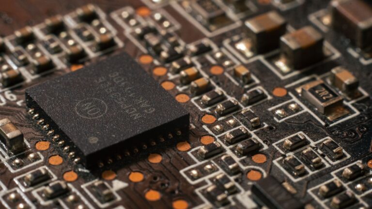
Artificial‑intelligence accelerators have become the workhorses of modern data centers, powering everything from large language models to real‑time image analysis. As model sizes explode and inference latency drops from seconds to milliseconds, the memory subsystem has emerged as the next frontier of performance. High‑Bandwidth Memory (HBM) is no longer a nice‑to‑have add‑on; it is a fundamental building block that enables AI chips to keep pace with the ever‑growing demand for data movement. This article explores why HBM matters, how it differs from traditional DRAM, and what design trade‑offs engineers face when integrating it into AI silicon.
The bandwidth bottleneck in AI workloads
Training a deep neural network involves feeding massive tensors—multi‑dimensional arrays of weights and activations—through layers that require billions of floating‑point operations per second. While compute units (matrix multiply engines, tensor cores, or systolic arrays) have become incredibly fast, they can only be as effective as the data they receive. In practice, the memory bandwidth between the chip’s compute fabric and its main memory often dictates the achievable throughput. When the data cannot be streamed fast enough, compute units sit idle, and the overall system performance stalls.
What makes HBM different?
HBM is a vertically stacked memory technology that places multiple DRAM dies on top of each other and connects them to the processor with a wide, high‑speed interposer or silicon‑through‑package (TSV) interface. This architecture yields three key distinctions compared with conventional DDR 4/5 modules:
- Massive parallelism: Each stack provides dozens of independent channels, delivering aggregate bandwidth measured in hundreds of gigabytes per second.
- Compact form factor: By stacking dies, HBM occupies far less PCB real‑estate, a critical advantage for dense accelerator cards and edge devices.
- Reduced power per bit transferred: The short, wide interconnects consume less energy than the long, narrow traces required for DDR memory.
These characteristics align closely with the needs of AI accelerators, which demand both high throughput and efficient power usage.
Bandwidth versus latency: why raw speed matters more for AI
Traditional computing workloads often prioritize low latency—think of a database query that must return results in microseconds. AI training and inference, on the other hand, are bandwidth‑bound. A single forward pass through a large transformer may require moving terabytes of activation data between layers. In this regime, the ability to stream data continuously outweighs the benefit of a few nanoseconds of lower latency. HBM’s wide bus architecture supplies the sustained data rates that keep tensor cores fed, while its relatively modest latency penalty is negligible in the context of massive data movement.
Scaling memory capacity without sacrificing speed
As models grow from millions to billions of parameters, the amount of on‑chip memory required for weights, activations, and intermediate results expands dramatically. Early AI chips paired a modest amount of HBM (e.g., 8 GB) with external DDR memory, but modern designs now integrate multiple HBM stacks, reaching capacities of 64 GB or more. Because each stack maintains its own high‑speed channels, adding more stacks scales bandwidth almost linearly. This modularity allows designers to balance capacity and performance based on target workloads, from edge inference with a single stack to large‑scale training with four or more stacks.
Power efficiency: the hidden cost of bandwidth
Data movement is a major source of energy consumption in AI systems. Studies have shown that moving a single bit of data off‑chip can consume orders of magnitude more energy than performing a floating‑point operation on that bit. HBM mitigates this issue in two ways. First, the short interconnects reduce the voltage swing and capacitance needed for each transfer, cutting per‑bit energy. Second, because HBM delivers more data per clock cycle, the memory controller can operate at lower frequencies while still meeting bandwidth demands, further lowering power draw. The net effect is a noticeable improvement in performance‑per‑watt—a critical metric for both data‑center operators and edge deployments where thermal headroom is limited.
Design challenges: integration, cooling, and cost
Despite its benefits, incorporating HBM into an AI accelerator is not trivial. The stacked nature of the memory requires a high‑density interposer or advanced packaging techniques, which increase manufacturing complexity and cost. Thermal management also becomes more demanding; the dense stack can trap heat, necessitating sophisticated cooling solutions such as vapor chambers or liquid cooling loops. Additionally, the memory controller logic must be tightly coupled with the compute fabric to exploit the full bandwidth, placing constraints on chip floor‑planning and verification cycles. Engineers must therefore weigh the performance gains against these practical considerations when deciding how much HBM to integrate.
Beyond HBM: emerging alternatives and the future landscape
While HBM currently dominates the high‑performance AI market, other memory technologies are emerging that could complement or even replace it in specific niches. Compute‑in‑memory approaches embed simple arithmetic directly within the DRAM array, reducing data movement altogether. Similarly, on‑chip SRAM caches designed for tensor operations can capture hot data, shaving bandwidth requirements. However, until these alternatives mature to the point where they can match HBM’s combination of capacity, bandwidth, and energy efficiency, HBM will remain the cornerstone of AI hardware design.
In summary, the relentless growth of AI models has turned memory bandwidth into a primary performance limiter. High‑Bandwidth Memory offers the parallelism, density, and power efficiency needed to keep modern AI chips fed with data at the speeds they require. While integration challenges and cost considerations keep HBM from being a universal solution, its advantages make it indispensable for any accelerator aiming to push the boundaries of deep‑learning performance.
