
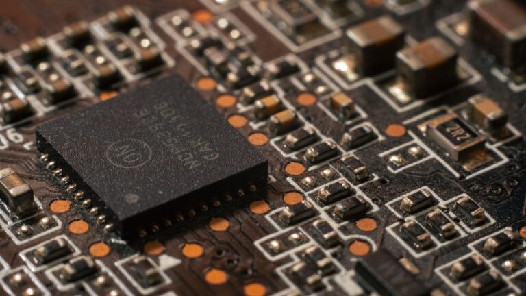
Understanding the Basics of Chiplet Technology
Chiplet technology is a design approach that assembles a complete processor or system‑in‑package (SiP) from multiple smaller silicon dies—called “chiplets”—instead of relying on a single monolithic die. Each chiplet can be fabricated using the process node that best matches its function, and the pieces are later interconnected with high‑density packaging technologies such as interposers, substrate routing, or advanced fan‑out wafer‑level packaging (FOWLP). The result is a modular system that can deliver high performance, better yields, and more flexibility in product development.
Why Chiplets Matter: Benefits Over Traditional Monolithic Designs
Several practical advantages have driven the industry’s shift toward chiplets. They are not just theoretical concepts; they address real challenges that semiconductor manufacturers have faced for years.
- Yield improvement: Smaller dies are less likely to contain defects, so the overall yield of a multi‑chiplet product is often higher than that of a comparably sized monolithic die.
- Process‑node optimization: High‑performance cores can be built on a leading‑edge node (e.g., 5 nm), while I/O, analog, or memory components can stay on a more mature, cost‑effective node.
- Design reuse and faster time‑to‑market: Chiplets that have already been qualified can be combined in new configurations, shortening the engineering cycle for next‑generation products.
- Scalability: Adding more compute or memory resources often means adding additional chiplets rather than redesigning an entire die.
A Brief History: From Concept to Commercial Reality
The idea of stitching together smaller silicon blocks dates back to the 1990s, when multi‑chip modules (MCMs) were used in high‑end servers. However, the modern incarnation of chiplets truly emerged in the 2010s with advances in high‑density interconnects. A notable milestone was AMD’s launch of the Zen 2 architecture in 2019, which used a central “core complex die” (CCD) paired with a separate I/O die fabricated on a 7 nm process. This was the first mainstream processor line to ship with chiplet‑based architecture at scale.
Intel followed suit with its “Foveros” technology, demonstrated in 2020 on the “Lakefield” processor that stacked a compute tile over an I/O tile using a 3‑D packaging method. Meanwhile, foundries such as TSMC and GlobalFoundries introduced advanced packaging solutions—CoWoS (chip‑on‑wafer‑on‑substrate) and InFO (integrated fan‑out)—that made high‑bandwidth, low‑latency connections between chiplets practical for mass production.
How Chiplets Are Connected: The Role of Advanced Packaging
The success of a chiplet design hinges on the interconnect technology that links the individual dies. The most common approaches include:
- Silicon interposers: Thin glass or silicon substrates with microscopic copper or polymer traces that route signals between chiplets, offering bandwidth comparable to on‑die connections.
- Embedded multi‑die interconnect bridge (EMIB): A small silicon bridge embedded in the package that provides a high‑density pathway for selected high‑speed links.
- Fan‑out wafer‑level packaging (FOWLP): An approach where the chiplets are placed on a redistribution layer that fans out the connections to a larger footprint, enabling fine‑pitch interconnects without a full interposer.
These technologies differ in cost, density, and thermal performance, so designers choose the one that aligns best with the target product’s performance envelope and price point.
Real‑World Examples: Chiplets in the Market Today
While the term “chiplet” may sound like a niche research topic, several products on store shelves already embody the concept.
AMD’s Ryzen 5000 series desktop CPUs and EPYC “Milan” server processors both use a multi‑chiplet architecture: multiple CCDs are attached to a single I/O die, delivering up to 64 cores in a single package. Intel’s “Alder Lake” desktop line, launched in 2021, combines performance cores built on a 10 nm node with efficient cores on the same die but uses a heterogeneous integration approach that shares many chiplet‑like characteristics. In the GPU arena, the upcoming “Radeon 7000” family is expected to employ chiplets to separate graphics cores from high‑bandwidth memory (HBM) stacks, a strategy that mirrors the approach taken by Nvidia’s recent data‑center GPUs.
Beyond CPUs and GPUs, networking ASICs and custom accelerators for AI workloads are increasingly adopting chiplet structures to blend specialized matrix‑multiply engines with general‑purpose logic and high‑speed transceivers.
Challenges and Trade‑offs: What Designers Need to Watch
Chiplet integration is not a silver bullet. Engineers must contend with several technical and economic hurdles:
- Signal integrity: Maintaining clean, high‑frequency signals across the interposer or substrate is more complex than on a monolithic die, especially for memory‑controller interfaces.
- Power delivery: Supplying consistent voltage to multiple dies while keeping the overall power budget low demands careful architecture of power planes and voltage regulators.
- Thermal management: Different chiplets may generate varying amounts of heat; efficient heat spreading and cooling solutions are essential to avoid hotspots.
- Design and verification complexity: The integration flow now includes packaging design, which requires new simulation tools and cross‑disciplinary expertise.
- Cost of advanced packaging: While chiplets can reduce silicon cost, the packaging steps—especially those involving silicon interposers—add expense that must be justified by the product’s performance or market positioning.
Addressing these issues often involves close collaboration between semiconductor designers, foundries, and packaging specialists, a trend that is reshaping the traditional silico‑centric development model.
The Road Ahead: Emerging Trends and Future Applications
Looking forward, chiplet technology is poised to play a central role in several emerging areas.
First, the drive toward heterogeneous computing—where CPUs, GPUs, AI accelerators, and specialized ASICs share a single package—fits naturally with a chiplet approach. By allowing each function to be built on its optimal process node, manufacturers can assemble highly tailored solutions without the cost of a one‑size‑fits‑all monolithic die.
Second, the rise of “chiplet ecosystems” is encouraging standardization. Industry groups such as the Open Compute Project and the OCP’s “Open Chiplet Interconnect” initiative are working on open specifications for chiplet interfaces, which could enable third‑party vendors to mix and match components much like building blocks.
Third, the increasing adoption of 3‑D stacking—where chiplets are placed directly on top of one another—offers even tighter integration. Stacked memory and compute chiplets can dramatically reduce latency, a benefit that is especially attractive for AI inference workloads that rely on rapid data movement.
Finally, as Moore’s Law slows, the economic incentives to maximize silicon utilization become stronger. Chiplets provide a path to continue performance scaling without the astronomical costs associated with ever‑larger monolithic dies.
In short, chiplet technology is not just a packaging novelty; it represents a strategic shift in how the semiconductor industry designs, manufactures, and markets complex silicon solutions. By leveraging modularity, process optimization, and advanced interconnects, chiplets enable higher yields, faster innovation cycles, and the flexibility needed for today’s heterogeneous computing demands.
