
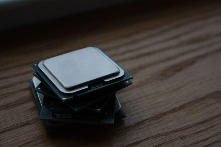
What is CPU Architecture?
When you turn on a computer, the central processing unit (CPU) is the heart that drives every computation. “CPU architecture” is a broad term that captures both the logical design of the processor—what instructions it understands and how it organizes its internal resources—and the physical implementation that turns those ideas into silicon. In practice, architects make choices about instruction sets, data paths, register files, cache structures, and power management, all of which determine how fast, efficient, and flexible a chip will be for the tasks you throw at it.
Instruction Set vs. Microarchitecture
The first layer of a CPU’s definition is the instruction set architecture (ISA). The ISA is a contract between software and hardware: it tells a compiler what binary patterns correspond to operations like addition, branching, or memory access. Popular ISAs include x86 (used by most PCs), ARM (dominant in mobile devices), and the open‑source RISC‑V, which is gaining traction in academia and industry.
Below the ISA sits the microarchitecture. This is the concrete engineering that implements the ISA’s abstract operations. Two different chips can share the same ISA yet have wildly different performance characteristics because they use distinct pipelines, cache strategies, branch predictors, and execution units. For example, Intel’s “Skylake” and AMD’s “Zen” families both speak x86, but each makes different trade‑offs between single‑thread latency and multi‑core throughput.
Key Components of a Modern CPU
While the exact layout varies, most contemporary processors contain a common set of building blocks:
- Registers: Small, fast storage locations that hold operands and intermediate results. General‑purpose registers (GPRs) are directly accessible by most instructions.
- ALU (Arithmetic Logic Unit): Performs integer arithmetic, bitwise logic, and simple shifts.
- FPU (Floating‑Point Unit): Handles real‑number calculations, often with specialized pipelines for multiplication, addition, and division.
- Decoder: Translates variable‑length machine code into fixed‑length micro‑operations (µops) that the execution engine can schedule.
- Scheduler / Issue Logic: Determines which µops can run in parallel, respecting data dependencies and resource limits.
- Cache hierarchy: A series of on‑chip memory layers (L1, L2, sometimes L3) that bridge the speed gap between registers and main memory.
- Control unit: Orchestrates the flow of data and instructions, often using finite‑state machines or more sophisticated micro‑code.
These components work together in a tightly choreographed dance, allowing a CPU to retire many instructions per clock cycle.
Pipelining and Parallelism
The most recognizable performance boost in modern CPUs comes from pipelining. By breaking instruction execution into stages—fetch, decode, execute, memory, and write‑back—a processor can have several instructions at different points in the pipeline simultaneously, much like an assembly line. When the pipeline is full, each clock tick can complete a new instruction, even though each individual instruction still takes multiple cycles to traverse the stages.
However, pipelines are vulnerable to hazards. A data hazard occurs when an instruction depends on the result of a preceding one that has not yet completed. To mitigate this, CPUs employ techniques such as:
- Out‑of‑order execution: reordering independent µops to keep the pipeline busy.
- Register renaming: eliminating false dependencies caused by reuse of the same architectural register.
- Speculative execution: guessing the direction of a branch and executing ahead, rolling back if the guess was wrong.
These mechanisms enable the processor to sustain high instruction‑throughput even in the presence of complex control flow.
Cache Hierarchy and Memory Access
Memory latency remains a dominant factor in overall system performance. To hide the millions‑of‑cycle delay of DRAM, CPUs embed a multi‑level cache hierarchy directly on the silicon die.
L1 cache sits closest to the core, typically split into separate instruction and data caches (I‑Cache and D‑Cache). It provides the fastest possible access, but its capacity is modest—often measured in tens of kilobytes. L2 cache offers a larger, slightly slower buffer, usually shared between the instruction and data streams of a single core. Some designs also include an L3 cache, a unified pool that can be shared across all cores on the chip, helping to coordinate data movement and reduce cross‑core contention.
Cache policies such as write‑back versus write‑through, and replacement algorithms like least‑recently‑used (LRU), determine how effectively the hierarchy serves the processor’s needs. Modern CPUs also incorporate prefetchers that predict future memory accesses based on patterns, issuing early loads to keep data ready before the core requests it.
Energy Efficiency and Modern Design Trends
Power consumption has become as critical as raw speed, especially in mobile devices and data centers where thermal constraints limit how fast a chip can run. Several architectural strategies address this challenge:
- Dynamic voltage and frequency scaling (DVFS): Adjusts clock speed and supply voltage on the fly, slowing the processor when full performance isn’t required.
- Big.LITTLE or heterogeneous cores: Combines high‑performance “big” cores with power‑efficient “little” cores, delegating light workloads to the latter.
- Clock gating: Turns off the clock signal to idle functional units, eliminating unnecessary switching activity.
- Specialized accelerators: Offloads tasks such as AI inference or video decoding to dedicated hardware blocks that consume far less energy per operation.
These techniques let a single chip span a wide performance envelope, from a few megahertz for background tasks to several gigahertz for demanding workloads, while staying within thermal design limits.
Future Directions: RISC‑V and Beyond
The landscape of CPU architecture continues to evolve. RISC‑V, an open‑source ISA, offers a modular approach where designers can add optional extensions for integer multiplication, atomic operations, or vector processing. Because the ISA is royalty‑free, it lowers the barrier for startups and academic groups to create custom silicon, fostering a more diverse ecosystem.
At the same time, industry players are exploring new ways to break the “frequency wall.” Chip‑level innovations such as chiplet integration—assembling separate dies for CPU cores, I/O, and memory controllers—allow manufacturers to mix and match proven components. Meanwhile, advances in 3‑D stacking, where memory and logic are bonded vertically, promise to shrink the distance between caches and cores, further reducing latency.
Beyond silicon, there is growing interest in alternative compute models. Neuromorphic architectures aim to emulate brain‑like processing, while quantum processors target specific algorithms that classical CPUs cannot solve efficiently. Even if these paradigms remain specialized, they influence mainstream CPU design by encouraging tighter integration of accelerators and more flexible instruction sets.
In sum, CPU architecture is a layered discipline that balances abstract instruction semantics with concrete hardware realities. Understanding the interplay between ISA, microarchitecture, pipelines, caches, and power management gives you a clearer view of why a laptop feels snappy while a server can handle thousands of simultaneous requests. As open standards like RISC‑V mature and new packaging technologies emerge, the next generation of processors will likely be more customizable, more energy‑aware, and more tightly integrated with the specialized engines that define today’s computing workloads.
