
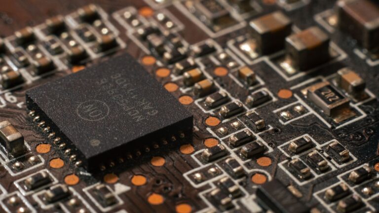
Artificial intelligence has moved from research labs to everyday devices, and the hardware that powers it—often called “AI chips”—has become a crucial piece of the puzzle. Unlike the general‑purpose processors that run most of our software, AI chips are engineered to handle the massive parallelism and data movement that modern machine‑learning models demand. Understanding how they work sheds light on why a smartphone can now translate speech in real time, why data centers can train huge language models faster than ever, and why new classes of edge devices can run sophisticated vision algorithms locally.
What Makes an AI Chip Different?
The primary distinction lies in purpose‑built circuitry. Traditional CPUs excel at a wide variety of tasks, switching quickly between different instruction streams. AI workloads, however, are dominated by a relatively narrow set of operations—most notably large matrix multiplications and tensor convolutions—that benefit from highly specialized execution units. By hard‑wiring these operations into silicon, AI chips achieve higher throughput while consuming less energy per operation than a CPU would.
Another key factor is the scale of parallelism. An AI model can contain billions of parameters that need to be multiplied and added together simultaneously. AI chips therefore contain thousands, sometimes millions, of tiny processing elements that work in concert, a design philosophy that would be inefficient and costly on a CPU designed for sequential instruction handling.
Core Architecture: From CPUs to GPUs to TPUs
Early AI research ran on CPUs, but as model sizes grew, the industry turned to graphics processing units (GPUs). GPUs were originally built for rendering images, a task that requires applying the same operation to many pixels at once—an ideal match for the parallel nature of neural‑network math. By repurposing GPUs for general computation (GPGPU), developers gained a massive speed boost for training deep networks.
Building on the GPU concept, companies introduced application‑specific integrated circuits (ASICs) such as Google’s Tensor Processing Unit (TPU). These chips strip away unnecessary features of a GPU and replace them with dedicated hardware for matrix math, further tightening the match between silicon and AI workloads. While GPUs remain popular for their flexibility and ecosystem, ASICs illustrate how tailoring the architecture to AI can unlock new performance and efficiency levels.
Specialized Building Blocks: Matrix Multipliers and Systolic Arrays
The heart of most AI chips is a matrix multiplication engine. Neural networks consist of layers that multiply input vectors by weight matrices, then add biases and apply non‑linear functions. To accelerate this, AI chips embed large arrays of multiply‑accumulate (MAC) units that can perform many operations in a single clock cycle.
One common implementation is the systolic array, a grid of processing elements that pass data rhythmically—like a heartbeat—through the array. Each element performs a MAC operation and forwards partial results to its neighbor, enabling the chip to keep data flowing without repeatedly reading from memory. This design reduces latency and maximizes data reuse, which is critical for energy efficiency.
- MAC Units: Perform the core multiply‑add step for every weight‑input pair.
- Systolic Arrays: Organize MACs into a pipeline that streams data with minimal buffering.
- Tensor Cores: Specialized MAC clusters found in modern GPUs that handle mixed‑precision operations.
- Vector Processors: Groups of ALUs that execute vectorized instructions on batches of data.
By arranging these blocks in a way that matches the mathematical structure of neural networks, AI chips can achieve orders of magnitude higher performance than general‑purpose processors.
Memory Hierarchy and Data Movement
Speed alone does not define an AI chip’s effectiveness; how it moves data is equally important. Neural‑network inference and training involve shuttling large tensors between on‑chip registers, fast SRAM caches, and external DRAM. Because accessing DRAM is far slower and more power‑hungry than on‑chip memory, modern AI chips employ a deep, multi‑level memory hierarchy.
At the lowest level, each processing element may have its own register file for immediate operands. Above that, shared SRAM buffers hold tiles of tensors that multiple units can access quickly. Some chips also integrate high‑bandwidth memory (HBM) directly on the package, shortening the distance between the processor and large memory pools. Efficient tiling and prefetching algorithms in the software stack help keep the compute units fed with data, preventing bottlenecks that would otherwise erase the benefits of raw arithmetic speed.
Power Efficiency and Thermal Management
Running thousands of MAC units at high frequency can generate significant heat. AI chips therefore adopt several strategies to stay within power budgets, especially for edge devices where battery life and cooling are limited. One approach is mixed‑precision arithmetic: using 16‑bit or even 8‑bit floating‑point formats for most calculations while retaining 32‑bit precision where accuracy is critical. Reducing the bit‑width cuts the amount of data moved and the energy per operation.
Another technique is dynamic voltage and frequency scaling (DVFS), which adjusts the chip’s power envelope based on workload intensity. On larger data‑center chips, sophisticated cooling solutions—such as liquid cooling plates—are used to dissipate heat efficiently, allowing the silicon to maintain peak performance without throttling.
Software Stack and Programming Models
Hardware alone does not deliver AI performance; developers need tools that translate high‑level models into hardware‑friendly code. Frameworks like TensorFlow, PyTorch, and ONNX provide graph representations of neural networks that can be optimized for a target chip. Backend compilers then map these graphs onto the chip’s primitives—splitting large matrix multiplies into tiles that fit the systolic array, inserting data‑movement instructions, and selecting the appropriate precision.
Many AI chips also expose low‑level libraries (for example, cuBLAS for GPUs or XLA for TPUs) that give developers fine‑grained control over kernel launches and memory allocation. This layered approach—from model definition to hardware execution—allows both researchers and production engineers to exploit the chip’s capabilities without writing silicon‑specific assembly code.
Future Directions and Emerging Trends
The rapid evolution of AI workloads continues to push chip designers toward new frontiers. One emerging trend is the integration of neuromorphic elements that mimic the brain’s event‑driven processing, potentially offering ultra‑low‑power inference for sparse data. Another area of interest is heterogeneous integration, where CPU, GPU, and AI‑specific accelerators share a single die or package, reducing latency and simplifying software stacks.
Finally, as models grow larger and more complex, researchers are exploring on‑chip training capabilities—allowing a device not only to run inference but also to adapt its parameters locally. Achieving this will require further innovations in memory bandwidth, precision handling, and algorithmic efficiency.
In sum, AI chips represent a convergence of architectural specialization, memory engineering, and software co‑design. By aligning silicon directly with the mathematical patterns of machine learning, they deliver the speed and efficiency that have turned AI from a curiosity into a mainstream technology.
